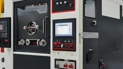
The market for thin film deposition systems is really picking up pace these days. I came across a report from MarketsandMarkets that says the global industry could hit around $12.2 billion by 2025, growing at about 7.2% annually. It’s pretty exciting—it seems all this growth is mainly fueled by new tech in semiconductor manufacturing and the rising demand for materials that deliver top-notch performance. Big names like AIXTRON, Veeco Instruments, and Applied Materials are really leading the charge here.
These thin film deposition systems are actually super important across different fields, like solar energy and optics. They give manufacturers the precise control needed over layer thickness, which really boosts how well these materials perform. That said, it’s not all smooth sailing. The production processes can be pretty complex, and high-end vacuum coating systems can be quite pricey, which makes it tough for smaller players to jump in. Finding ways to tackle these hurdles is definitely key if we want more folks to get involved.
To keep this momentum going, continuous innovation and new tech investments are a must. Collaborations between research centers and industry giants could really help push things forward. And it’s crucial that newcomers understand both what these systems can do and where their limits are—getting that balance right can make all the difference. Overall, navigating this competitive scene thoughtfully will be essential if we’re serious about long-term growth and success in this field.

Top Global Thin Film Deposition Systems: Market Overview and Trends
The global thin film deposition systems market is witnessing significant growth. According to recent reports, the market is projected to reach USD 28 billion by 2025, with a CAGR of around 7.5%. This growth is driven by advancements in technology and increased demand in applications such as electronics and photovoltaics. Countries in Asia-Pacific are leading in production, accounting for 40% of the global market share. The region’s robust electronics manufacturing sector heavily utilizes Thin Film Deposition Equipment.
A noticeable trend is the shift towards more sustainable practices. Companies are investing in eco-friendly thin film deposition technologies. This is in response to regulatory pressures and the increased importance of sustainability in manufacturing processes. Yet, challenges remain, including the high costs associated with advanced systems and the need for ongoing maintenance. As a result, some companies may overlook the importance of upgrading their thin film deposition equipment, which could hinder their competitive stance in the market.
Another emerging trend is the integration of automation in thin film deposition processes. Organizations are exploring innovative technologies to enhance efficiency. The adoption of AI and IoT is rising, yet not all firms are leveraging these advancements. This creates a potential gap in performance compared to more technologically adept competitors. Overall, continual adaptation and investment in thin film deposition equipment is essential for companies wishing to thrive in this evolving landscape.
Critical Factors in Choosing Thin Film Deposition Technologies: A Buyer’s Guide
When selecting thin film deposition technologies, several critical factors must be considered. The application and material requirements often dictate the choice of technique. Different technologies, such as Physical Vapor Deposition (PVD) and Chemical Vapor Deposition (CVD), offer varying levels of precision and efficiency. According to industry reports, the global thin film deposition market is expected to grow at a compound annual growth rate (CAGR) of 6.4% from 2021 to 2028. This growth underscores the importance of making informed decisions regarding technology selection.
Another key consideration is the scalability of the thin film deposition system. Buyers must evaluate whether the equipment can meet future production demands. A report by Transparency Market Research indicates that companies seek systems that can easily adapt to changing market conditions. This adaptability can be crucial as industry standards evolve.
Cost efficiency also remains a major concern. While advanced technologies may promise higher yields, initial investments can be significant. Balancing upfront costs with long-term benefits is essential. Some systems may require extensive maintenance or specific environmental controls, impacting overall operational costs. Understanding these nuances can aid buyers in making well-rounded decisions.
Comparison of Physical and Chemical Vapor Deposition Techniques for Efficiency
When it comes to thin film deposition, two primary techniques dominate the field: physical vapor deposition (PVD) and chemical vapor deposition (CVD). Both methods have their strengths and limitations, which makes understanding them essential for global buyers. PVD often excels in material purity and adhesion. It uses physical processes to deposit thin films, making it ideal for applications requiring hard and durable coatings. However, achieving uniform thickness can sometimes be challenging.
CVD, on the other hand, is known for its ability to cover complex shapes and provide excellent uniformity. This method relies on chemical reactions to form films, which can result in lower defect densities. Yet, it can have longer processing times and higher operational costs. Each technique has its place in the marketplace, and the choice often depends on specific applications and material requirements.
Consider these factors: the required film thickness, the substrate material, and the desired properties of the final coating. Reflection on potential trade-offs is important. Buyers should evaluate how each method aligns with their production goals.
It's crucial to align your technology choice with your application needs. Think about scalability and processes. What works for a small batch may not suit large-scale production. Making informed decisions can lead to more efficient production techniques and better end products.
Emerging Thin Film Deposition Systems: Innovations and Market Demand
Innovations in Thin Film Deposition systems are reshaping industries, driven by market demand. A recent report from industry analysts indicates the global thin film deposition market will reach approximately $27 billion by 2025, reflecting a CAGR of 8.5%. This growth is significantly influenced by technological advancements in semiconductors and renewable energy sectors.
Emerging thin film deposition systems boast a range of novel techniques. These include atomic layer deposition, which allows for single-atom precision . This level of precision is critical for creating advanced materials used in electronics. Additionally, recent innovations have led to more cost-effective processes, making thin film deposition accessible to smaller enterprises. However, challenges remain, such as high equipment costs and maintenance complexities.
Implementing thin film deposition methods can yield better product performance . Manufacturers should consider exploring new techniques while balancing potential costs. Regular evaluations can identify effective methods and technologies. Adopting a continuous improvement mindset will ensure companies enhance their thin film deposition capabilities sustainably.
Key Players in the Thin Film Deposition Market: Profiles and Market Share
In the thin film deposition market, key players are essential for understanding industry dynamics. These companies contribute significantly to innovation and market share. They utilize various technologies, such as physical vapor deposition and chemical vapor deposition, to create thin films for multiple applications.
To navigate this complex market, consider the following. Look for companies with a proven track record in research and development. A robust portfolio can signal reliability. Additionally, examine their customer relationships. Strong partnerships often lead to improved service and product support.
Market share can fluctuate. Keep an eye on emerging players who may disrupt the status quo. These newcomers often bring fresh ideas. However, established firms have experience and resources. Balance risk with opportunity. Understanding both segments can guide better investment decisions.
Future Growth Prospects for Thin Film Deposition Systems in Various Industries
The future for thin film deposition systems appears promising across various sectors, fueled by advancements in technology and increasing demand. According to a recent market report, the global thin film deposition market is expected to reach $30 billion by 2026, with a compound annual growth rate (CAGR) of 6.5%. This growth is particularly driven by industries such as electronics, solar energy, and healthcare.
In the electronics sector, the demand for smaller, more efficient components is surging. Thin film deposition plays a critical role in producing semiconductors and microchips. The solar industry is also experiencing significant changes, with thin film solar panels becoming more viable and efficient. Reports indicate that thin film technology could capture up to 30% of the solar energy market by 2025.
While the prospects are bright, challenges remain. The need for improved techniques and methodologies is apparent. Many manufacturers still encounter issues with uniformity and scalability in deposition processes. Furthermore, environmental concerns regarding certain materials used in thin film deposition cannot be overlooked. Continuous innovation and adherence to sustainability are essential. Stakeholders must engage in thoughtful practices to ensure future growth aligns with industry standards.
Impact of Thin Film Coatings on Energy Efficiency and Sustainability Practices
Thin film coatings play a vital role in enhancing energy efficiency and promoting sustainable practices. These coatings improve the performance of various surfaces, including solar panels and windows. By reducing the amount of energy absorbed and lost, they significantly increase efficiency. For instance, reflective coatings on solar panels can boost energy capture by minimizing heat loss.
Moreover, thin films contribute to sustainability efforts by reducing material waste. They allow for less bulk material to be used while maintaining performance. However, there is a challenge in balancing the application process with environmental considerations. The manufacturing of these materials often involves complex procedures that can generate hazardous waste. This prompts the need for more eco-friendly methods.
As industries prioritize green practices, innovation in thin film technologies will likely drive significant changes. The market demands adaptability and efficiency while also pushing for less environmental impact. Continuous research is needed to address these concerns while maximizing the benefits of thin film applications. There is much to reflect on in making production processes cleaner.
Exploring the Advantages and Applications of China TLC Series Anode Layer Ion Source Coating Machines in Thin Film Deposition
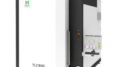
The TLC series anode layer ion source coating machines represent a significant advancement in thin film deposition technology, effectively blending Magnetron Sputtering (MS) with state-of-the-art anode layer ion source capabilities. This innovative equipment is specifically designed to enhance the quality and performance of coatings across various industrial applications. Featuring a unique cold cathode gas ion generation mechanism, the anode layer ion source delivers a robust ion beam current while ensuring remarkable stability, making it an ideal choice for manufacturers seeking precision in their deposition processes.
One of the standout applications of the TLC series is in the deposition of Diamond-Like Carbon (DLC) coatings. These coatings are renowned for their low internal stress, outstanding hardness, exceptional wear resistance, and minimal friction properties. As a result, DLC coatings are increasingly favored in demanding sectors such as automotive, precision tooling, medical equipment, and aerospace components. Additionally, the TLC series accommodates a broad spectrum of materials, allowing for tailored solutions to meet diverse industry needs, ensuring that users can achieve optimal results regardless of their specific requirements.
In addition to its superior coating performance, the TLC series is engineered with efficient process control in mind, promoting environmental sustainability and cost-effectiveness. This combination of high-performance capabilities and a commitment to sustainability positions the TLC series as a preferred choice for modern surface engineering applications, paving the way for innovative advancements in various engineering domains.
FAQS
: The market is growing due to technological advancements and rising demand in electronics and photovoltaics.
The Asia-Pacific region leads, accounting for 40% of the global market share in production.
Companies invest in eco-friendly deposition technologies to align with sustainability goals and regulatory demands.
High costs for advanced systems and ongoing maintenance often challenge companies’ growth and equipment upgrades.
Automation enhances efficiency, but not all companies are adopting innovations like AI and IoT, creating performance gaps.
They improve surfaces like solar panels by reducing energy loss, enhancing overall energy capture significantly.
Thin films reduce material waste and allow less bulk material use while maintaining performance standards.
The complex production processes often generate hazardous waste, highlighting the need for cleaner methods.
Look for proven R&D capabilities and strong customer relationships, which indicate reliability and better support.
Continuous investment in technology and adapting to market demands are crucial for maintaining competitiveness.
Conclusion
The article "Top Thin Film Deposition Systems for Global Buyers" explores the current landscape of thin film deposition systems, focusing on market trends and emerging technologies. It provides a comprehensive market overview, highlighting critical factors that buyers should consider when selecting deposition technologies, including efficiency and application-specific requirements.
Furthermore, it contrasts physical and chemical vapor deposition techniques, examining their efficiency and suitability for different uses. The article also delves into innovative thin film deposition systems that are gaining traction, driven by market demand. Key players in the industry are analyzed to understand their market share and influence, while future growth prospects across various industries and the impact of thin film coatings on energy efficiency and sustainability practices are discussed, emphasizing the vital role of thin film deposition systems in advancing technological and environmental objectives.