• icon_youtube
  • Linkedin
  • Leave Your Message
    0%

    Picking out the right thin film deposition system in 2026 is more than just checking the chamber size or the price tag. Today, manufacturers in semiconductors, displays, solar, and optics really need sharper control over film thickness, cleaner interfaces, and shorter downtime for maintenance. I mean, SEMI reported that in 2024, global sales of semiconductor manufacturing equipment hit about $117 billion — that’s a huge investment in these high-tech tools. But honestly, spending a lot on equipment doesn't automatically mean you'll get better films in the end.

    So, here’s the thing — take a closer look. You should consider things like the temperature range of the substrate, how stable the vacuum is, how uniform the plasma is, how efficiently the target material gets used, and whether it has in situ monitoring. Even a small five-degree drift in temperature can make a big difference in the stress levels, how well films stick, or their crystal structure. Pump-down times matter too — especially if you’re running hundreds of wafers a day. And according to IDTechEx’s research on thin-film electronics, there’s increasing pressure to develop flexible substrates, transparent conductors, and processes that work at lower temperatures. These new applications often demand different system setups compared to traditional silicon manufacturing.

    John A. Thornton, a pretty renowned sputtering expert, once said, “The structure of sputtered coatings is determined by the substrate temperature and the argon pressure.” That quote from his 1974 paper in the Journal of Vacuum Science & Technology still rings true today, since the physics behind the process is pretty much the same and still limits what’s possible. So, when you’re looking at vacuum coating systems, don’t just go by fancy brochures — ask for real data. Ask for uniformity maps, contamination info, maintenance records, and references from other clients. Seeing is believing. And remember, the system needs to match your material stack, throughput needs, and operator skills. Here’s a little uncomfortable truth, though — the ‘best’ system isn’t always universal. If you’re mainly doing high-speed metal layers, a tool optimized for that might tank when it comes to reactive oxides or delicate polymer films. Basically, choosing the right system is an ongoing process — keep testing, documenting, and stay open to changing your mind as you learn more.
    How to Choose Thin Film Deposition Systems in 2026?

    Define Thin Film Deposition Goals and Material Requirements

    Choosing a thin film deposition system in 2026 should begin with the film, not the equipment catalog. Define the target thickness, acceptable uniformity, deposition rate, substrate temperature, and production volume. A laboratory optical coating may need nanometer-level control, while a protective layer may prioritize adhesion and throughput. Write the application in measurable terms. High quality is not measurable.

    Material requirements narrow the process window. List the film chemistry, substrate type, surface roughness, thermal sensitivity, and allowable contamination. Some materials demand reactive gases, controlled stoichiometry, or very low base pressure. Others fail when energetic particles create stress, heating, or poor adhesion. For multilayer stacks, check interface stability rather than judging each layer alone. A film can look excellent today. It may crack.

    During system comparisons, request data from conditions resembling your process. Ask for thickness maps, repeatability results, particle counts, and maintenance records. Independent metrology is valuable because an instrument reading can hide edge effects. Measure the surface. Leave room for uncertainty in the specification. An early target may be too optimistic. I would rather record a failed trial than quietly adjust the acceptance limit. That decision protects later scale-up, where small material variations can become costly process drift.

    Compare Deposition Technologies for Different Film Applications

    Choosing Thin Film Deposition Equipment in 2026 requires matching the process to the film’s real function.

    Semiconductor layers often demand atomic-scale control, making ALD suitable for uniform barriers and high-aspect-ratio structures. CVD can provide faster coverage for dielectric films. PVD remains practical for conductive layers when throughput and material utilization matter.

    SEMI’s World Fab Forecast, published in 2024, projected global semiconductor manufacturing equipment spending above 110 billion dollars in 2025. That forecast signals continued pressure for stable uptime, not merely impressive specifications.

    Solar modules need a different balance. Large-area sputtering and PECVD systems support conductive oxides, absorbers, and passivation layers.

    The IEA PVPS Trends 2024 report recorded global photovoltaic capacity exceeding 1.4 terawatts by the end of 2023. Such scale makes chamber size, target utilization, and maintenance time commercially important.

    Optical coatings may favor evaporation or ion-assisted deposition, especially when low absorption and precise reflectance are required. Flexible packaging needs low-temperature processing, often with plasma-enhanced methods or spatial ALD.

    In my experience, the cheapest tool is rarely the lowest-cost choice. A five-minute cleaning delay can become hours across multiple chambers.

    Ask for film uniformity maps, defect data, recipe repeatability, and measured cost per coated area. Laboratory data can mislead. Production reality is harsher.

    Also examine substrate sensitivity, thermal budget, precursor handling, and future material changes. A system optimized for one film may become restrictive when customer specifications shift.

    Evaluate System Performance, Uniformity, and Process Control

    Choosing a deposition system in 2026 requires more than a specification sheet. Thin Film Deposition Techniques must be judged through measured stability, not advertised capability. SEMI’s 2024 World Fab Forecast placed global fab equipment spending near US$112 billion for 2025. That scale raises the cost of small process errors. Ask for within-wafer thickness maps, wafer-to-wafer drift, particle-add data, and recovery time after maintenance. Numbers matter.

    Uniformity should be tested across the usable area, not only at the center point. Request raw data from edge exclusion zones and patterned wafers. A 1% average error can hide sharp edge roll-off. Compare sheet resistance, optical constants, stress, and composition after repeated runs. The IRDS 2024 roadmap continues to identify process variability and defect control as critical challenges for advanced devices. Evaluate distributions, not single values. Short tests can mislead.

    Process control deserves equal weight. Check endpoint sensing, mass-flow response, chamber matching, recipe permissions, alarms, and automatic fault recovery. The system should record timestamps, sensor traces, calibration status, and operator changes. Use statistical process control with limits based on real production data. Do not accept repeatability claims without sample size and confidence intervals. Ten excellent wafers are not a factory. In pilot work, ask whether uniformity survives chamber seasoning, target aging, and overnight idle periods. I would also score uptime and maintenance labor, because a stable process that is rarely available is only partly useful. Review the evidence with process, maintenance, and quality engineers—not one evaluator.

    How to Choose Thin Film Deposition Systems in 2026? - Evaluate System Performance, Uniformity, and Process Control
    Evaluation Dimension Recommended Benchmark What to Measure Preferred Evidence Why It Matters Typical Risk if Overlooked 2026 Selection Priority
    Film Thickness Uniformity ≤ ±2% across a 200 mm substrate; ≤ ±3% across a 300 mm substrate Within-substrate and wafer-to-wafer thickness variation Mapping data from at least 5 production-size substrates Directly affects optical response, electrical resistance, etch depth, and device yield Edge-to-center variation, non-uniform device performance, and increased rework Very High
    Deposition Rate Stability Long-term rate drift within ±1–2% during a production run Instantaneous rate, average rate, and rate drift over time Quartz crystal monitoring, optical monitoring, or calibrated in-situ sensors Stable rates improve thickness repeatability and reduce process corrections Thickness errors caused by source aging, thermal drift, or plasma instability Very High
    Thickness Repeatability ≤ 1% three-sigma variation for a qualified recipe Run-to-run and lot-to-lot thickness variation Statistical process-control charts covering multiple production runs Shows whether the system can maintain a qualified process over time Unpredictable product characteristics and excessive process tuning Very High
    Process Pressure Control Stable pressure control over the recipe operating range; typically below 1 × 10⁻⁵ Torr for high-vacuum evaporation and approximately 1–20 mTorr for magnetron sputtering Base pressure, operating pressure, pressure recovery, and gas-flow response Calibrated capacitance manometers, ion gauges, mass-flow controllers, and trend logs Pressure influences mean free path, film density, stress, stoichiometry, and contamination Porous films, unstable plasma, composition drift, and poor adhesion Very High
    Substrate Temperature Control Uniformity within ±3–5°C across the substrate, subject to the process temperature Setpoint accuracy, thermal uniformity, heating rate, and cooling behavior Calibrated thermocouples, pyrometers, or temperature-sensitive test wafers Controls crystallinity, stress, density, grain structure, and adhesion Film cracking, delamination, poor optical properties, or substrate damage Very High
    Plasma or Power Stability Power and reflected-power fluctuation typically below 1% during steady state Forward power, reflected power, current, voltage, arc frequency, and plasma impedance Logged generator data and arc-management performance during extended runs Important for sputtering and plasma-assisted processes that depend on stable ion energy Particles, arcing defects, pinholes, non-uniform deposition, and target damage High
    In-Situ Endpoint Detection Automated endpoint capability with recipe-to-recipe thickness error ≤ 1–2% Optical emission, optical interference, quartz crystal, or plasma endpoint signals Correlation between in-situ signals and ex-situ metrology Reduces dependence on fixed-time recipes and compensates for source or target aging Over-deposition, under-deposition, and unnecessary material consumption High
    Material Compatibility Validated process window for the required metals, dielectrics, semiconductors, or multilayers Source temperature, reactive-gas compatibility, target size, and cross-contamination controls Film composition, adhesion, roughness, and contamination test results Prevents material-specific failures during scale-up or product changeover Cross-contamination, source poisoning, poor stoichiometry, or premature component wear Very High
    Film Stress Control Process-specific target; commonly less than ±300 MPa for sensitive multilayer structures Compressive or tensile stress before and after thermal cycling Wafer-curvature measurements using a calibrated stress-analysis method Stress affects wafer bow, overlay accuracy, cracking, peeling, and long-term reliability Delamination, substrate distortion, fractured films, and assembly problems High
    Particle Performance Defined particle limit based on substrate size and application; trend should remain stable over qualification runs Particle count by size class, defect density, and particle source location Dark-field inspection, surface scanning, witness substrates, and chamber inspections Particles are a major source of shorts, pinholes, optical defects, and yield loss Random catastrophic defects and difficult-to-trace yield excursions Very High
    Automation and Recipe Control Recipe version control, interlocks, audit trail, user permissions, and automated data logging Parameter limits, alarm handling, recipe edits, and lot traceability Control-system demonstration and sample production-history reports Improves repeatability, operator independence, compliance, and root-cause analysis Unauthorized changes, incomplete records, and operator-induced variation Very High
    Metrology Integration Direct data connection to thickness, sheet-resistance, optical, stress, and surface-defect measurements Data transfer, calibration status, measurement frequency, and SPC integration Demonstration of closed-loop or semi-closed-loop process control Shortens feedback cycles and supports predictive process maintenance Delayed detection of drift and dependence on manual data transcription High
    Maintenance and Uptime Documented preventive-maintenance intervals and stable availability target above 90% after qualification Mean time between failures, mean time to repair, cleaning time, and consumable life Service records, maintenance procedures, and spare-parts availability data Determines effective production capacity and total cost of ownership Unplanned downtime, missed delivery schedules, and inconsistent chamber conditions High
    Scalability and Throughput Capacity matched to substrate size, batch size, cycle time, and expected annual demand Useful deposition time, pump-down time, loading time, and changeover time Cycle-time study using the intended substrate format and process sequence Prevents a system that meets laboratory specifications but cannot support production volume Capacity bottlenecks, excessive labor, and high cost per coated substrate High
    Energy and Process Efficiency Quantified energy use per substrate or per deposited thickness, including pumps, heaters, plasma, and cooling Electrical power, process-gas consumption, material utilization, and cooling demand Utility measurements collected during representative production recipes Supports operating-cost control and increasingly important environmental reporting Higher operating cost, oversized utilities, and avoidable material waste Medium–High
    Qualification and Data Integrity Complete recipe, calibration, alarm, maintenance, and batch-history records Timestamp accuracy, access control, backup, electronic signatures, and audit trails Sample data package and documented qualification protocol Enables traceability, process validation, and reliable comparison between development and production Unverifiable results, slow investigations, and difficulty reproducing qualified processes High
    Benchmark values are representative engineering targets rather than universal specifications. Final acceptance limits should be established from the required film material, substrate size, layer stack, device tolerance, and validated production process.

    Assess Substrate Compatibility and Chamber Configuration

    When choosing a thin film deposition system in 2026, start with the substrate, not the tool brochure. SEMI’s 2024 World Fab Forecast tracks more than 1,400 semiconductor facilities and production lines globally. This diversity demands careful compatibility checks. Ask whether the system supports silicon, glass, metal foil, polymer, or compound semiconductor substrates. Their thermal limits can differ sharply.

    Measure substrate size, thickness, warpage, and coefficient of thermal expansion. A polymer panel may deform under a metal’s deposition temperature. Glass can tolerate heat, yet its surface may develop stress cracks during cooling. Review vacuum outgassing, particle sensitivity, surface charging, and plasma exposure. Test real coupons. Small samples often hide edge effects. They should not.

    Chamber configuration directly affects repeatability. Compare batch and single-substrate designs, then examine load-lock capacity, source geometry, target-to-substrate spacing, and substrate rotation. A larger chamber may improve throughput but increase pump-down time and material consumption. SEMI’s 2024 semiconductor equipment outlook projected industry equipment spending above 100 billion US dollars, showing the scale of investment behind these decisions. Still, spending more does not guarantee better films. Film thickness maps, stress measurements, and adhesion results should guide selection. The IRDS 2023 roadmap also emphasizes tighter process control as dimensions shrink. Leave room for recalibration. Real production rarely behaves like the first qualification run.

    How to Choose Thin Film Deposition Systems in 2026?

    Assess Substrate Compatibility and Chamber Configuration

    Representative room-temperature coefficients of thermal expansion (CTE) are shown in µm/m·K. A smaller CTE generally reduces thermal-stress risk when the deposited film and substrate experience heating or cooling during deposition.

    Use low-stress chucking and controlled heating for low-CTE substrates such as silicon and borosilicate glass. For higher-CTE materials such as stainless steel and polyimide, prioritize temperature uniformity, flexible fixturing, and chamber configurations that support gradual thermal ramping. Actual values vary with material grade, temperature, and supplier specifications.

    Review Automation, Safety, Maintenance, and Scalability

    Choosing Thin Film Deposition systems in 2026 requires more than comparing chamber size or advertised rates. In pilot runs, operators notice small delays first: recipe loading, substrate alignment, and recovery after a failed cycle. A useful system records each parameter automatically, including pressure, temperature, gas flow, and operator changes. Clear dashboards help engineers detect drift before a coating batch is wasted. Automation should support judgment, not hide it. That distinction matters.

    Safety begins with physical design. Interlocked doors, leak detection, exhaust monitoring, and controlled access reduce routine exposure risks. Emergency controls should remain understandable during a noisy alarm. I prefer systems with maintenance zones that are easy to reach without disturbing nearby equipment. Training records, fault logs, and calibration reminders also strengthen accountability. A polished interface cannot compensate for weak ventilation or confusing procedures.

    Maintenance costs often appear after installation. Ask how quickly pumps, seals, sensors, and fixtures can be inspected and replaced. Modular layouts can shorten downtime, although they may introduce more connection points and new failure modes. Plan for future substrates, larger loads, and additional process modules without rebuilding the entire line. Capacity claims deserve practical testing. A system that runs beautifully for one week may behave differently under continuous production. Leave room for doubt, review service data, and revise the specification when evidence disagrees with the original plan.

    Calculate Total Cost of Ownership and Select the Best System

    Choosing Thin-Film Deposition equipment in 2026 requires more than comparing purchase prices. SEMI’s December 2024 World Fab Forecast projected global semiconductor manufacturing equipment spending at approximately $112.8 billion in 2025. That investment pressure makes cost discipline essential. Build a ten-year Total Cost of Ownership model before requesting quotations. Include installation, facility upgrades, gases, targets, power, cooling water, labor, software, service contracts, downtime, and disposal. The spreadsheet should show cost per deposited square meter, not only the equipment price.

    The practical test is a production simulation. Record chamber clean time, pump-down duration, deposition rate, target utilization, and first-pass yield. A system costing $900,000 may outperform a $650,000 alternative if it saves six hours weekly and reduces failed batches. Calculate annual cost using realistic electricity tariffs and maintenance intervals. The U.S. Department of Energy’s Industrial Decarbonization Roadmap identifies energy efficiency as a major lever for industrial cost and emissions reduction. Measure power at the tool, not from a brochure.

    That is the trap.

    Ask operators to inspect the chamber, load samples, and recover from a minor alarm. ISO 14644 controls cleanroom conditions, but it does not guarantee process stability. Require service-response terms, spare-parts availability, and documented acceptance tests. The model will be imperfect. Material prices change, and utilization forecasts can be optimistic. Recalculate quarterly after pilot production. Thin-Film Deposition selection should reward reliable output, measurable uptime, and transparent operating costs.

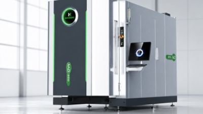
    MD200 Arc Coating Equipment: Compact Ion Plating Systems from Leading China Suppliers and Factories

    The MD200 Arc Coating Equipment is a compact ion plating system designed for suppliers and factories in China that require flexible, reliable coating performance within a limited production space. Its compact structure makes it well suited to small-batch manufacturing, non-standard tools, and resharpened tools that may require specialized handling. By supporting in-house coating operations, the system can help manufacturers improve process control, reduce dependence on outside services, and respond more efficiently to varied customer requirements.

    Equipped with four arc sources, the MD200 provides adaptable coating capability for different tool geometries and production needs. Its WET lateral hot filament etching function supports effective surface preparation before deposition, helping promote coating consistency and adhesion when processing challenging tool surfaces. The system is practical for factories seeking repeatable results without investing in a large-scale production line, while its compact format allows easier integration into existing workshops. For tool suppliers, machining businesses, and production facilities handling frequent resharpening or customized orders, the MD200 offers a balanced combination of process flexibility, efficient operation, and dependable coating quality.

    FAQS

    : How should deposition system performance be evaluated?

    : Request thickness maps, wafer-to-wafer drift, particle data, and maintenance recovery time. Numbers matter. Do not rely on advertised capability alone.

    Why is full-area uniformity testing important?

    Measure the usable wafer area, including edge exclusion zones and patterned wafers. Averages can hide sharp edge roll-off. Compare thickness, resistance, optical properties, stress, and composition across repeated runs.

    How many samples are needed for reliable repeatability claims?

    Ask for sample size, variation ranges, and confidence intervals. Ten excellent wafers are not a factory. Short tests can mislead.

    Which process-control features should a system include?

    Check endpoint sensing, gas-flow response, chamber matching, alarms, and automatic fault recovery. The system should record pressure, temperature, timestamps, calibration status, and operator changes.

    How can automation support production decisions?

    Clear dashboards should show sensor traces and gradual process drift. Automation should support judgment, not hide it. Review records before approving a recipe change.

    What safety and maintenance details deserve attention?

    Check interlocked doors, leak detection, exhaust monitoring, controlled access, and clear emergency controls. Inspect pumps, seals, sensors, and fixtures during a practical demonstration. A polished interface cannot fix weak ventilation.

    How should total cost of ownership be calculated?

    Build a ten-year model covering installation, utilities, gases, materials, labor, software, service, downtime, and disposal. Measure power at the equipment. Calculate cost per deposited square meter, not only purchase price.

    How can competing systems be compared fairly?

    Run a production simulation with chamber cleaning, pump-down, deposition rate, material use, and first-pass yield. A cheaper system may cost more after repeated failures. The model stays imperfect.

    How should future scalability be tested?

    Test larger loads, future substrates, continuous operation, and additional process modules. Modular layouts may reduce downtime but add connection points. Leave room for doubt.

    Conclusion

    Choosing the right thin film deposition systems in 2026 begins with clearly defining the desired film properties, including material type, thickness, conductivity, optical performance, adhesion, and production volume. These requirements help determine whether physical, chemical, thermal, or hybrid deposition methods are most suitable for the application. Buyers should compare deposition technologies according to film quality, process flexibility, throughput, uniformity, and compatibility with sensitive materials or complex structures.

    A complete evaluation should also cover system performance, process monitoring, substrate size and shape, chamber configuration, automation, operator safety, maintenance needs, and future scalability. Reliable control of temperature, pressure, gas flow, and deposition rate is essential for repeatable results. Finally, purchasing decisions should be based on total cost of ownership, including equipment, utilities, consumables, labor, maintenance, downtime, and possible upgrades. The best system is not always the one with the lowest initial price, but the one that delivers consistent film performance, efficient operation, and long-term value for the intended application.

    Charlotte

    Charlotte

    Charlotte is a dedicated marketing professional at Guangdong HUASHENG Nanotechnology Co., Ltd., a leading domestic supplier of advanced nanocoating solutions. With an exceptional depth of knowledge in the company’s innovative product offerings, Charlotte plays a pivotal role in bridging the gap......
    Previous Top Thin Film Deposition Systems for Global Buyers?